
Environmental management of exhaust gases associated with the manufacture of semiconductors
Ever considered the environmental impact of a computer? A phone? Or even just the silicon chips inside them? The semiconductor industry is a $375 billion (1) business, and the manufacturing of silicon chips creates a great deal of waste. One key set of chemicals used in the processes are Fluorinated Greenhouse Gases (F-GHGs). Here we will explore the F-GHG usage and the carbon dioxide equivalent (CO2e) footprint of the factories that make them.
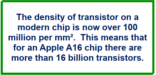
Semiconductors are devices that when an increasing voltage is applied to them, will begin to conduct electricity. Usually made from silicon, by varying the electrical properties, transistors (an electrical switch) can be manufactured. Over the past 40 years Moore's law, named after Gordon Moore the co-founder and CEO of Intel, has meant that the number of transistors in an integrated circuit has doubled every two years. This has been achieved by continual process development to shrink the size of transistors, such that the most modern chips now have a density of over 100 million transistors per square millimetre and that a processor such as the Apple A16, which is used in the latest iPhone 14 Pro, has more than 16 billion transistors (2).
The other major use for semiconductors is memory and the amount of memory required is increasing exponentially. According to Forbes, 90% of the world's data was generated in the last two years with 2.5 million terabytes data being created each day. In 2014 less than 0.1 zettabytes (1021 bytes) had been generated whereas the forecast for 2024 is that over 90 zettabytes of data will be generated.
The other major use for semiconductors is memory and the amount of memory required is increasing exponentially. According to Forbes, 90% of the world's data was generated in the last two years with 2.5 million terabytes data being created each day. In 2014 less than 0.1 zettabytes (1021 bytes) had been generated whereas the forecast for 2024 is that over 90 zettabytes of data will be generated.
|
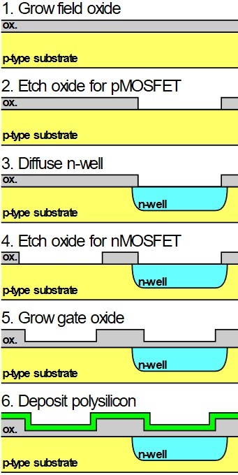
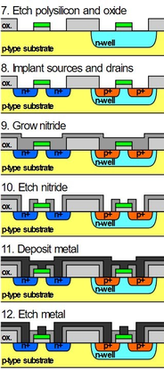
Semiconductor Manufacturing
The simplistic view of semiconductors manufacturing is a cycle of depositing material onto silicon, patterning (lithography) and, then etching.
The deposition process uses some F-GHGs in order to maintain the cleanliness of the processing chamber as deposited material can contaminate the next wafer. The etch processes use a great deal of different F-GHGs to create the fine structures for circuitry. These F-GHGs can have high Global Warming Potentials (GWP) and long lifetimes in the atmosphere as seen in Table 1. An example is CF4, which has a 100 year GWP of 7,380 compared to 1 from CO2.
|
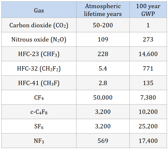
Table 1. Global Warming Potentials (3).
|
|
According to US Environmental Protection Agency's Facilities Level Information on Greenhouse gases Tool (FLIGHT) (4), the emission of the F-GHGs for a modern semiconductor fabrication plant can be in excess of 500,000 tons CO2e. However, the semiconductor industry has long recognised the potential impact of F-GHGs and has, over the last 25 years, strived to reduce the emissions of these gases. An example was The World Semiconductor Council, which agreed in 1999 to reduce emissions by 10% by 2010 (5). They have employed strategies such as optimization of processes, substitution of non- (or low-) GWP gases and particularly abatement, where the destruction of some of these gases can be particularly challenging. This means that emissions can be reduced by 90%. So, what does that mean for our environmental footprint of phones? The iPhone 14 Pro has a lifecycle carbon footprint of 63 kg CO2e of which 81% is from the production process (6). Increasing the memory from 128 GB to 512 GB increases the footprint to 84 kg CO2e; however, increasing to 1TB and it becomes 116 kg CO2e. Thus, the importance of reduction of F-GHGs in the semiconductor manufacturing process is paramount
|
|
References
1. VLSI Research. The Chip Insider 2020
2. Wikipedia. Apple Silicon. Wikimedia Foundation, 10 January 2023. https://en.wikipedia.org/wiki/Apple_silicon (Accessed 12.01.2023)
3. Masson-Delmotte, V., P. Zhai, A. Pirani, S. L. Connors, C. Péan, S. Berger, N. Caud, Y. Chen, L. Goldfarb, M. I. Gomis, M. Huang, K. Leitzell, E. Lonnoy, J.B.R. Matthews, T. K. Maycock, T. Waterfield, O. Yelekçi, R. Yu and B. Zhou (eds.). Summary for Policymakers. In: Climate Change 2021: The Physical Science Basis. Contribution of Working Group I to the Sixth Assessment Report of the Intergovernmental Panel on Climate Change. IPCC, Cambridge University Press. 2021 In Press. https://www.ipcc.ch/report/ar6/wg1/chapter/summary-forpolicymakers/
4. US Environmental Protection Agency. Facilities Level Information on Greenhouse gases Tool (FLIGHT) . https://www.epa.gov/ghgreporting (Accessed 12.01.2023)
5. Tsai, W. T., Chen, H. P., & Hsien, W. Y. (2002). A review of uses, environmental hazards and recovery/recycle technologies of perfluorocarbons (PFCs) emissions from the semiconductor manufacturing processes. Journal of Loss Prevention in the Process Industries, 1 5 ( 2 ), 65 - 75 . https://doi.org/10.1016/ S0950-4230(01)00067-5
6. Apple Inc. Product Environmental Report. iPhone 14 Pro. Report, 2022.
https://www.apple.com/environment/pdf/products/ iphone/iPhone_14_Pro_PER_Sept2022.pdf
Royal Society of Chemistry Environmental Chemistry Group
Burlington House
Piccadilly London W1J 0BA |
|
© COPYRIGHT 2022. ALL RIGHTS RESERVED.
Website by L Newsome
|